ABOUT US
- home
- ABOUT US expand_more
Vision & Goals
Vision
Leading the semiconductor market through next-generation chiplet technology
Goal
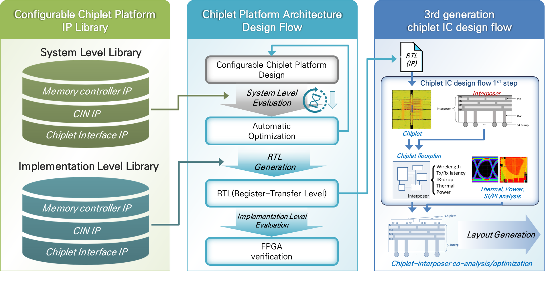
Developing a P&P chiplet integration framework to advance chiplet platform design productivity


- This center aims to lead the semiconductor market through next-generation chiplet technology, and to achieve this, we intend to conduct research in the fields of IP, Architecture, and Methodology, which are core to next-generation chiplet technology.
- To maximize chiplet platform design productivity, we aim to provide a connection base between chiplet suppliers and chiplet platform designers through IP acquisition, and to establish a design framework system capable of automatic generation of network models between chiplet dies and performance evaluation of the built chiplet platform.
- To establish a chiplet design framework system, we set the following core technologies as the goals of our research and development :
- Customized chiplet integration methodologies for chiplet standard interfaces
- Chiplet design and integrated circuit verification flows
- Electrical modeling of interconnection/PDN and SI/PI analysis techniques
- Transaction-level chiplet platform performance evaluation metrics analysis framework
- Chiplet transceiver IP technology supporting chiplet standard interfaces
- DRAM/SRAM memory controller IP design considering chiplet standard interfaces
- Configurable CIN designs supporting system-level performance evaluation
- Shared cache structures capable of efficiently processing data access for multiple chiplets
- Designs for high-reliability/high-yield chiplet testing/repair circuits