RESEARCH
- home
- RESEARCH expand_more
IP
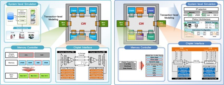
Level 1 : Development of SystemC-based Transaction-Level Modeling(TLM) framework for designing and evaluating the chiplet transceiver IP and the memory controller supporting the chiplet standard interfaces
Level 2 :
Development of the memory controller IP that supports high reliability/low power/low process design variation chiplet interface technology and various memory access scheduling/cache policies
Development of simulation framework that can evaluate/analyze the performance of chiplet systems based on various IP combination
Level 1
Level 2
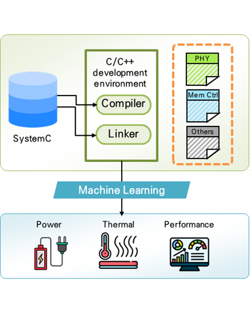
IP modeling for inter-chiplet simulation and development of machine learning-based system level evaluation/verification framework
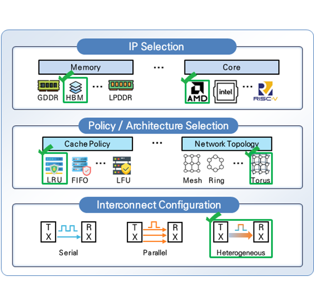
Development of algorithms optimizing IP combinations, based on TLM simulation and system level evaluation for reconfigurable 3rd generation chiplet systems
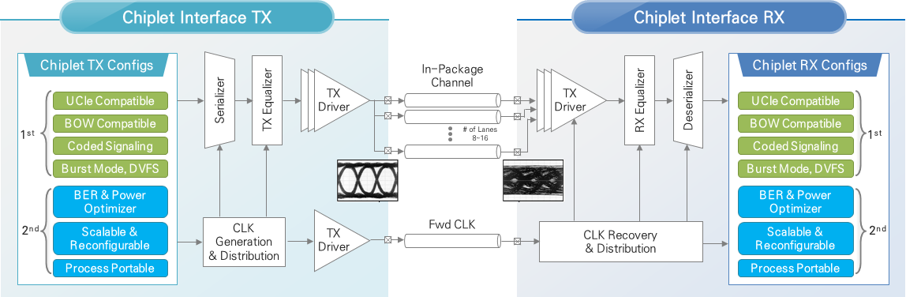
Development of high energy efficiency/low delay interface IP for next generation heterogeneous semiconductors ( UCIe, Bow )
Development of technology for designing chiplet interface with high reliability/low power/low process design variation applicable to various chiplet systems
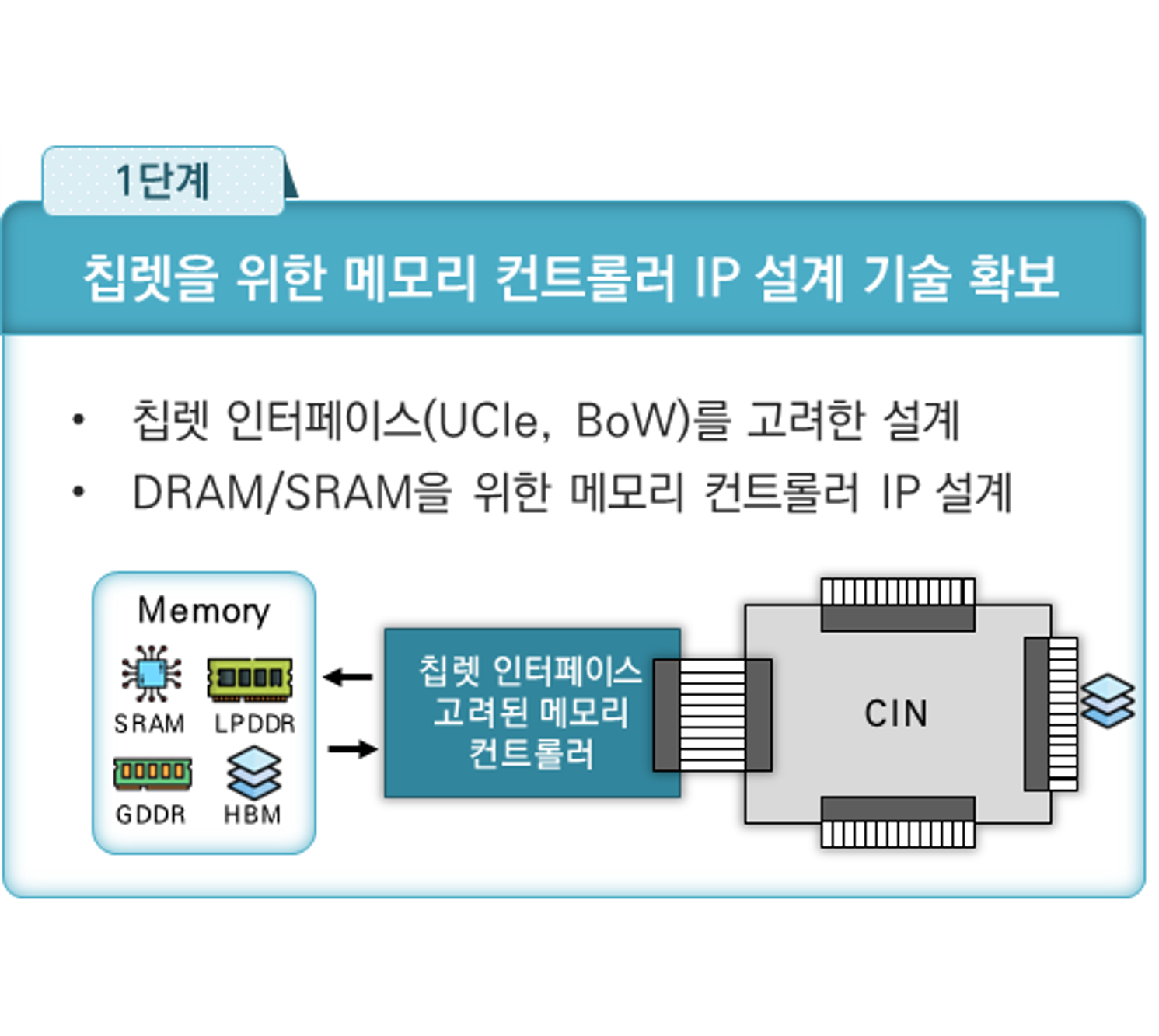
Designing original technology for memory controller IP design solutions to standardize chiplet die design
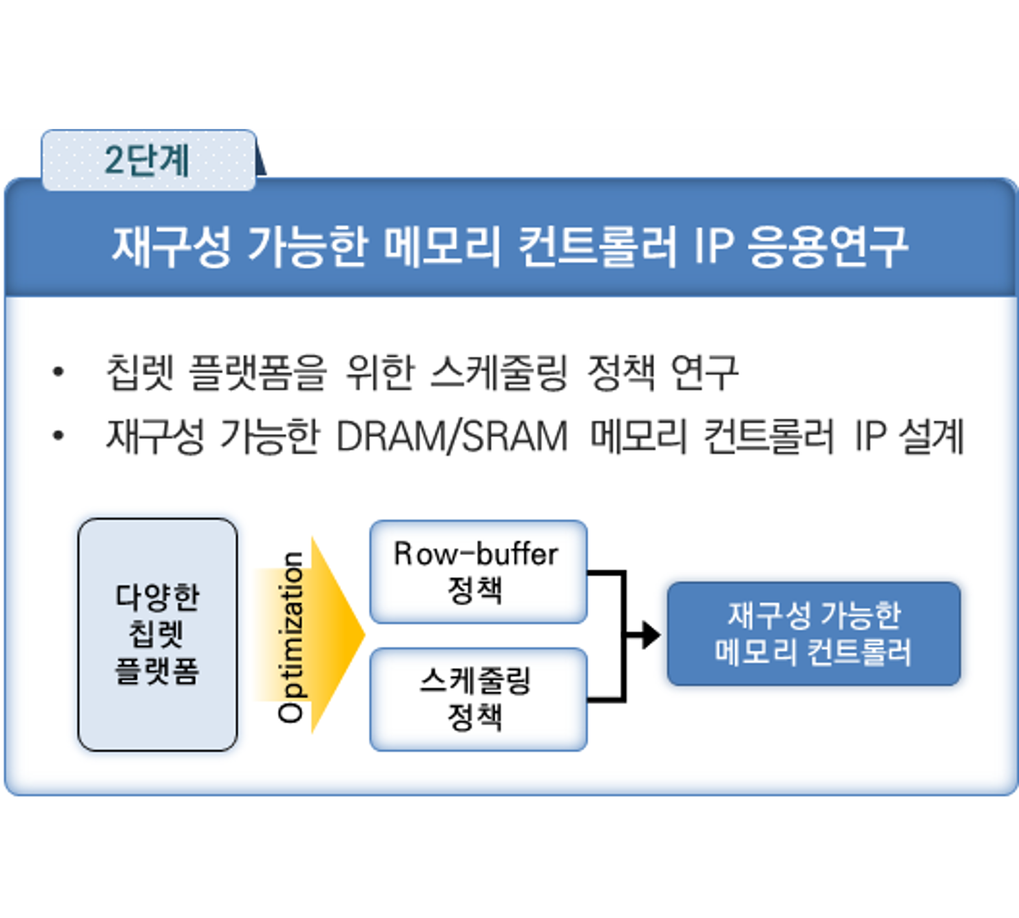
Applied research on reconfigurable memory controller IP for the chiplet platform